

 contact@canrd.com
 +86 18928276992
 Home/Resources/Knowledge/Testing&Analysis/What Do SEM, TEM, EDS & EBSD Measure? Battery Material Characterization Guide
What Do SEM, TEM, EDS & EBSD Measure? Battery Material Characterization Guide
Canrd August 18, 2026 131
Introduction
When a battery electrode suffers particle cracking, abnormal particle morphology, poor coating integrity, impedance rise or unexpected capacity fade, the very first question should not be:
Should I run SEM or TEM?
A far more productive starting point is:
What evidence do I need to verify or rule out my suspected failure mechanism?
SEM, ESEM, TEM, EDS and EBSD all rely on electron‑matter interactions, yet each delivers distinct types of information. Some capture surface topography; others map elemental distribution; some resolve nanoscale interfaces and lattice structures; while others quantify crystal orientation and local strain.
In battery research, these tools deliver maximum value when deployed against well‑defined engineering problems and combined with electrochemical, bulk structural and chemical evidence.
CANRD frames microscopic characterisation as one link within the complete R&D workflow:
Animal property → GTD subsets → MTX I & ITS
This methodology avoids over‑reliance on isolated microscopy results. Failure analysis at CANRD integrates non‑destructive inspection, electrochemical diagnosis and component‑level disassembly analysis to build complete evidence chains for material‑, electrode‑ or cell‑level faults.
1. Technique Selection: Start from Your Battery Engineering Question
Instead of memorising instrument specifications, match your analytical target to the most suitable technique.
| Analytical Target | Primary Technique | Typical Battery‑Related Use‑Case |
|---|---|---|
| Observe particle / electrode surface topography | SEM‑SE | NCM secondary particle cracking, graphite particle morphology, electrode delamination, separator surface contamination |
| Identify compositional differences across regions | SEM‑BSE | Detect foreign inclusions, secondary phases, metallic contamination on electrodes |
| Locate spatial distribution of target elements | SEM-EDS/TEM-EDS | Contamination identification, separator coating distribution, current‑collector residue, elemental mapping of active material particles |
| Investigate intra‑particle features and nanoscale interfaces | TEM | Cathode surface coating layers, silicon‑carbon composite interfaces, internal particle defects |
| Measure lattice spacing and local crystal features | HRTEM / SAED | Surface modification layers, phase boundaries, local structural degradation upon cycling |
| Characterise grain orientation and texture | EBSD | Copper / aluminium foil, tab welding zones, metallic casing, metallurgically driven battery component failures |
| Analyse insulating / moisture‑sensitive samples incompatible with high vacuum | ESEM | Polymer components, separators, selected moisture‑retaining specimens |
Key takeaway: SEM, TEM, EDS and EBSD are not hierarchical “better‑or‑worse” alternatives. They capture fundamentally different physical signals.
2. Why the Same Electron Beam Generates Diverse Signals: Interaction Volume Fundamentals
When a focused electron beam bombards a solid sample, scattering takes place within a 3‑dimensional electron‑sample interaction volume beneath the sample surface. Different analytical signals originate from different depths inside this volume.
- Secondary electrons mainly originate from the near‑surface layer and are highly sensitive to surface geometry.
- Backscattered electrons come from a deeper interaction zone.
- Characteristic X‑rays for EDS are generated from an even larger volume.
This explains a commonly observed laboratory phenomenon:
An SEM secondary‑electron image can exhibit sharp fine features, while the EDS elemental map acquired on exactly the same field‑of‑view shows noticeably poorer spatial resolution.
The size of interaction volume is governed by accelerating voltage, material density & atomic number, beam parameters and sample geometry. Published resolution figures for SEM, EDS and EBSD represent typical operating ranges, not fixed universal specifications. Real‑world effective resolution always depends on instrument setup and sample conditions.
3. SEM: Routine Workhorse for Particle and Electrode Morphology
What SEM can reveal
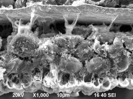
SEM is usually the first microscopy tool deployed for battery samples, balancing relatively large observation areas with micron‑to‑nano feature resolution. Typical investigation questions include:
- Are cathode secondary particles cracked after long‑term cycling?
- Does graphite exhibit severe particle agglomeration?
- Are abnormal particle clusters present in silicon‑carbon anodes?
- Is active material coating peeling away from current collectors?
- What is the cross‑sectional structure of coated electrodes?
- Are deposits or foreign particles found on separator surfaces?
Within CANRD’s failure‑analysis practice, SEM is routinely used to characterise anode and cathode morphology post controlled teardown, observing active‑particle integrity and electrode microstructure.
Secondary Electron (SE) vs Backscattered Electron (BSE) imaging
SE Imaging: Signal dominated by near‑surface secondary electrons. Optimised for surface morphology observation: cracks, surface roughness, particle shapes and fracture surfaces.
BSE Imaging: Signal intensity correlates strongly with average atomic number of sample regions; heavier‑element domains appear brighter. BSE enables fast screening for foreign metallic particles, second‑phase precipitates and compositionally heterogeneous zones.
Important limitation: BSE brightness contrast cannot directly identify elemental species. Confirmation requires EDS or complementary chemical characterisation.
4. Common Pitfall: What SEM Alone Cannot Prove
A frequent mistake in battery failure diagnosis is drawing definitive root‑cause conclusions purely from SEM micrographs.
For instance:
“A bright particle is visible → this must be iron contamination.”
SEM (including BSE contrast) cannot confirm elemental identity independently.
Another typical logical leap:
“NCM particles show cracking → particle cracking is the root cause of capacity loss.”
SEM can confirm cracking exists, but cannot prove it is the causal source of performance decay.
A validated evidence chain would look like:
- SEM: Confirm particle cracking morphology
- EDS / chemical analysis: Examine local elemental composition
- XRD / TEM: Evaluate associated structural degradation
- EIS / dQ/dV / cycling datasets: Electrochemically verify performance degradation matches the observed microstructure
This aligns with CANRD’s analytical philosophy: morphology, crystal structure, chemical composition and electrochemical testing must be cross‑checked; no single micrograph constitutes final proof for failure root causes.
5. ESEM: For Samples Unsuitable for Conventional High‑Vacuum SEM
Environmental SEM (ESEM) runs under controlled gas‑vapour ambient instead of strict high‑vacuum conditions for conventional SEM. Its major benefit: certain insulating samples can be observed without conductive sputter‑coating pre‑treatment.
For battery research, ESEM is applicable for selected polymer materials, separators, insulating composites and moisture‑containing specimens.
Nevertheless, ESEM isnot an “upgraded better SEM”Compared with optimized high‑vacuum SEM, environmental operation compromises imaging resolution and signal‑to‑noise ratio.
One critical battery‑specific note: cycled electrodes and fragile interfacial films are highly sensitive to air exposure, moisture and sample transfer. In many scenarios preserving native interface status outweighs the convenience of coating‑free ESEM observation. Sample characterisation strategy should follow your scientific objective and sample sensitivity, rather than only considering sample conductivity.
6. TEM: Dig Deeper When SEM Cannot Resolve Nanoscale Localised Problems
SEM excels at locating abnormal features across electrode or particle scale. TEM is deployed when you need to analyse nanoscale internal details inside those regions.
Since electrons must transmit through the specimen, TEM requires ultra‑thin electron‑transparent samples; sample preparation is substantially more labour‑intensive.
Typical battery TEM use‑cases:
- Nanometer-scale surface coatings on cathode particles
- Silicon Carbon Compiler
- Intra‑particle damage induced by cycling
- Local crystal defects and phase boundaries
- Nano‑sized reaction‑induced interfacial layers
Within CANRD’s material evaluation and failure‑analysis capability matrix, TEM complements SEM, XRD and compositional tools for both cathode and anode material investigation.
7. Distinguish TEM, HRTEM and SAED: They Answer Different Crystal‑Structure Questions
TEM comprises multiple operating modes for different analytical goals.
- Bright‑field TEM: Observe internal microstructure, grain boundaries, dislocations and nano‑precipitates.
- HRTEM (High‑Resolution TEM): Resolve lattice fringes to measure interplanar spacing, identify crystalline domains, lattice distortion, coherent / incoherent phase interfaces.
- SAED (Selected‑Area Electron Diffraction): Acquire diffraction patterns from micro‑sized local regions to extract crystallographic information: discrete spots for single crystals, concentric rings for polycrystalline material, diffuse halos for poorly‑ordered domains.
HRTEM and SAED provide local micro‑zone crystal information, which complements bulk XRD:
XRD reflects the average crystal status of bulk material.TEM characterises crystal information of a tiny specific region.
Neither technique replaces the other; they work synergistically.
8. Critical Limitation: TEM Results Are Not Automatically Representative of Bulk Samples
TEM’s strength is also its major constraint: it probes an extremely small area of an ultra‑thin lamella.
At high‑quality HRTEM image is confirmed:
This nanoscale structure exists within this local sampling area.
It cannot automatically conclude:
This feature exists across the whole material batch.
This consideration is highly relevant for heterogeneous battery materials: secondary‑particle cathodes, partially coated particles, silicon‑containing composites and cycled electrodes with localised degradation.
Robust research workflow combines large‑area statistical observation with high‑resolution local evidence: SEM first assesses how widespread a feature is across the sample, then TEM delivers detailed nanoscale structural insight for representative locations.
9. EDS: Identify Elements and Their Spatial Distribution
EDS detectors can be fitted to both SEM and TEM instruments. When high‑energy electrons strike atoms inside samples, characteristic X‑rays are emitted; X‑ray energy enables elemental identification. Three standard operating modes:
- Point analysis: Element composition at a single spot
- Line scan: Composition variation across an interface
- Elemental mapping2‑D spatial distribution of target elements over the field‑of‑view
Practical experience from CANRD reverse‑engineering projects illustrates the correct collaboration logic: SEM locates morphological anomalies; EDS identifies associated elemental information, e.g. separator contamination analysis.
SEM pinpoints where the feature is; EDS reveals what elements are associated with it.
10. Why EDS Maps Appear Blurrier Than Corresponding SEM Images
Poor EDS map resolution is often misattributed to detector performance. The root cause lies in electron‑sample interaction volume differences.
Secondary‑electron signals that form high‑resolution SEM images originate from an ultra‑thin near‑surface layer. The X‑rays detected in EDS are generated within a much larger interaction volume.
As a result: SEM imaging resolution ≠ EDS mapping spatial resolution.
Reducing accelerating voltage can shrink interaction volume to some extent, yet simultaneously alters X‑ray excitation efficiency. Optimisation requires trade‑offs rather than simply applying the lowest possible voltage. Always interpret EDS spatial resolution considering accelerating voltage, sample thickness, material composition, detector geometry and whether you are performing SEM‑EDS or TEM‑EDS.
11. What Conventional EDS Cannot Measure
EDS delivers powerful elemental information, yet several key chemical properties lie outside its capability scope:
- Oxidation state: Detecting nickel cannot distinguish Ni²⁺, Ni³⁺ or other valence states.
- Chemical bonding: Detecting fluorine cannot differentiate LiF, PVDF or other fluorinated species.
- High‑sensitivity trace‑level quantification: Trace‑element quantification typically requires ICP and other bulk analytical tools.
- Routine lithium mapping: Conventional EDS is not suited for lithium distribution measurement.
For this reason, CANRD's full material‑analysis workflow supplements SEM‑EDS with XRD, ICP‑AES, EPMA, TOF‑SIMS, NMR and other techniques selected according to investigation targets.
12. SEM-EDS vs TEM-EDS
The physical principle of EDS remains identical for SEM and TEM platforms, but sample geometry changes interaction volume dramatically.
For bulk samples in SEM, electron beams interact with a relatively large volume, limiting spatial resolution. In TEM, specimens are ultra‑thin lamellae, so interaction volume shrinks significantly. TEM‑EDS achieves far higher localised elemental resolution, ideal for nano‑coatings, fine precipitates, thin interfaces and individual nano‑particles.
Bear in mind the representativeness constraint again: high‑resolution TEM‑EDS mapping reflects only a tiny local zone and cannot be generalised to the entire material batch without statistical support.
13. EBSD: Crystal‑Orientation Information Beyond Morphology and Elemental Analysis
EBSD is fundamentally a crystallographic‑orientation characterisation technique. The sample is tilted relative to electron beam; diffracted backscattered electrons produce Kikuchi diffraction patterns, which are indexed to calculate local crystal orientation.
EBSD outputs include IPF orientation maps, grain‑size statistics, grain‑boundary distribution, misorientation statistics, texture data and KAM maps.
Clear conceptual distinction versus EDS:
EDS answers: What elements exist here?EBSD answers: How are crystal lattices oriented here?
14. Practical Battery‑Engineering Scenarios for EBSD
EBSD is not a routine first‑choice for most active‑material powder analysis. It adds high value for components governed by metallurgical and mechanical behaviour:
- Copper / aluminum runs
- Grain structure of tab materials
- Laser‑welded or ultrasonic‑welded tab zones
- Metallic casing material
- Mechanically deformed conductive battery components
- Fracture and recrystallisation analysis
CANRD’s R&D and failure‑analysis platform covers not only active electrode materials but also current collectors, welding joints and other structural cell parts. EBSD is deployed when failure hypotheses point toward mechanical‑metallurgical root causes instead of purely electrochemical degradation.
15. Interpreting KAM (Kernel Average Misorientation)
KAM calculates average crystallographic misorientation between one measuring point and its neighbouring points. Elevated KAM values indicate orientation gradients associated with plastic deformation, lattice curvature and accumulated local strain. It serves as an indirect metric for deformation and geometrically‑necessary dislocations.
Important note: KAM is not direct visualisation of individual dislocation lines. If direct observation of dislocation structures is required, TEM remains the appropriate technique. Converting KAM values into absolute dislocation density without solid pre‑defined assumptions will lead to over‑interpretation.
16. Common Causes for Low EBSD Indexing Rate
Poor indexing performance usually originates from sample surface quality rather than intrinsic material properties. Typical root causes:
- Surface damage induced by polishing
- Excessive surface roughness
- Surface oxidation or surface contamination
- Heavy plastic deformation
- Ultra‑fine grain size
- Overlapping diffraction patterns
EBSD signals originate from an extremely shallow near-surface region; damage-free surface preparation is essential for obtaining usable Kikuchi patterns.
17. Technique Overview: Compare by Information Output
Avoid memorising nominal resolution parameters which vary heavily with instrument configuration and sample conditions. Focus instead on what each tool delivers, its sampling characteristics and inherent limitations.
| Technique | Core Information | Sampling Characteristic | Main Limitations |
|---|---|---|---|
| SEM‑SE | Surface topography & morphology | Large field‑of‑view, surface‑sensitive | No direct composition or lattice information |
| SEM‑BSE | Atomic‑number based contrast | Near‑surface region | Contrast cannot identify chemical species |
| ESEM | Morphology under gaseous ambient | Surface observation | Lower imaging performance vs high‑vacuum SEM |
| TEM | Internal nano‑scale microstructure | Highly local sampling | Demanding sample prep, limited representativeness |
| HRTEM / SAED | Lattice fringe & local crystallography | Extremely local sampling | Strong dependence on sample orientation and thickness |
| EDS | Element identification & distribution | Determined by SEM / TEM geometry | Cannot measure oxidation state / chemical bonding |
| EBSD | Crystal orientation, grain boundaries, texture | Near‑surface crystallography | Requires high‑quality damage‑free sample surface |
18. Evidence‑Driven Characterisation Planning for Battery Failure Analysis
Following CANRD's failure‑analysis workflow, characterisation starts from visual inspection, electrical performance test and non‑destructive examination, followed by controlled disassembly. Analyse cathode, anode, separator, electrolyte and current‑collector components targeted at your failure hypothesis, rather than running all available tests blindly.
Scenario 1: Rapid capacity fading of cycled cathode
- SEM: Compare morphology between fresh and aged electrodes, check particle cracking and surface deposits
- EDS: Detect elemental enrichment or contamination on abnormal zones
- TEM / HRTEM (if required): Investigate surface reconstruction, coating integrity and internal nano‑structural degradation
- XRD: Confirm bulk crystal‑structure changes
- EIS / electrochemical diagnosis: Verify whether observed microstructure matches impedance rise and capacity loss behaviour
Final conclusion is built on cross‑correlated multi‑source evidence, not a single SEM micrograph.
Scenario 2: Fast degradation of silicon‑carbon anode
- SEM: Evaluate electrode cracking, particle agglomeration and morphological degradation
- TEM / HRTEMCharacterize silicon-carbon internal structure and nano-interfaces
- TEM‑EDS (as needed): Confirm nanoscale elemental distribution
- Electrochemical testing: Correlate microstructural evolution with ICE, swelling, impedance and cycling performance
This workflow aligns with CANRD’s core logic: material characterisation must connect with electrode manufacturing parameters and real cell performance.
Scenario 3: Unknown foreign particle observed on electrode
- SEM‑SE: Locate the abnormal particle
- BSE: Screen for atomic‑number contrast
- EDS point analysis & mapping: Identify associated elemental composition
- ICP (when bulk trace‑contamination quantification is needed)
This workflow is far more robust than deducing contamination purely from BSE brightness.
Scenario 4: Tab / current‑collector mechanical failure
- SEM: Observe fracture morphology and welded‑zone microstructure
- EDS: Screen local composition and surface contamination
- EBSD: Grain orientation analysis, recrystallization, and local misorientation (where applicable)
- TEM (only when direct observation of nano‑defects / dislocations is required)
EBSD delivers far higher practical value at initial stage than TEM for metallurgically driven faults.
19. You Do Not Need Every Characterisation Tool for Every Sample
Running all available characterisation tests does not guarantee solid conclusions; it often generates redundant data. Always design your test matrix around your failure hypothesis.
- If investigating electrode delamination: prioritise cross‑section SEM, coating morphology and manufacturing process review.
- If verifying cathode surface coating existence: HRTEM plus compositional analysis become key.
- If tracing origin of foreign metallic particles: SEM‑BSE EDS serve as effective primary screening.
- If researching abnormal deformation / recrystallisation of aluminium foil near welds: EBSD is more valuable than TEM for initial screening.
This hypothesis‑driven approach eliminates unnecessary testing and ensures each dataset contributes toward validating or rejecting assumptions.
20. Electron Microscopy Is Only One Link Within the Full Battery Evidence Chain
CANRD’s complete R&D and pilot‑validation system extends well beyond electron microscopy. Analytical capabilities also cover XRD, BET, thermal analysis, GC‑MS, ICP and a full suite of electrochemical testing platforms, with specialised techniques deployed according to project requirements.
Reliable root‑cause investigation requires multi‑dimension evidence:
- Morphology: AM / IS
- Elemental distribution: EDS mapping
- Crystal structure: XRD / SAED
- Surface & interfacial chemistry: Surface‑sensitive analytical techniques
- Bulk composition: ICP / XRF
- Electrochemical performance consequence: Capacity, EIS, cycling, rate capability, dQ/dV
- Gas & electrolyte decomposition products: GC‑MS and related tools
Trustworthy root‑cause conclusions are achieved when independent measurement results converge to support one failure mechanism.
FAQ
Q1: Core difference between SEM and TEM?
SEM is optimized for large‑area surface morphology and electrode‑scale inspection. TEM requires electron‑transparent thin samples and provides high‑resolution information on local nano‑scale internal structures, interfaces, and crystal defects. The two techniques are complementary and cannot substitute for one another.
Q2: EDS versus EBSD?
EDS identifies elemental species and their spatial distribution. EBSD measures crystal orientation, grain boundaries and texture. EDS answers “what elements are here”; EBSD answers “how are crystals oriented here”.
Q3: Why is my SEM image sharp but EDS mapping blurry?
Secondary‑electron signals for SEM imaging are generated within an ultra‑thin near‑surface layer. X‑rays for EDS come from a larger electron‑sample interaction volume, hence mapping resolution is inherently lower than SE image resolution.
Q4: Can EDS determine element oxidation state?
No. Conventional EDS identifies elements, yet cannot directly obtain chemical valence or bonding information.
Q5: Can EBSD directly image individual dislocations?
No. KAM indicates regions with accumulated local strain, yet cannot resolve individual dislocation lines. TEM is required to directly observe dislocation structures.
Q6: When should I select ESEM instead of conventional SEM?
ESEM fits selected insulating, uncoated or moisture‑containing samples incompatible with high‑vacuum conditions. Select it based on sample stability and analytical goals, rather than treating it as a universal replacement for high‑vacuum SEM.
Conclusion
Instrument selection for battery electron microscopy should never be decided purely based on “which tool has higher resolution” or “which instrument is more advanced”. Each technique answers distinct scientific questions:
- SEM: Reveal surface and electrode‑level morphology
- TEM / HRTEM: Uncover nanoscale internal microstructure and lattice‑scale interfacial features
- EDS: Identify elements and their spatial distribution
- EBSD: Characterise crystal orientation, grain boundaries and local misorientation
- ESEM: Alternative ambient imaging for special samples unsuitable for high‑vacuum environment
For battery R&D and failure diagnosis, real analytical power comes from combining microscopic data with electrode manufacturing context, cell testing results and controlled‑teardown observations.
CANRD’s R&D philosophy links material characterisation, slurry‑electrode process development, prototype cell validation and failure diagnosis together. Microscopic characterisation is not an isolated lab output.
Previous
Single Crystal vs Po...Related Products & Services
Use Canrd products and R&D services to turn battery knowledge into practical experiments.
Coin Cell Case
ProductCoin cell cases for validating materials and electrochemical concepts from the article.
Use coin cell cases in your next test →Sodium Electrolyte
CategoryElectrolytes for sodium-ion battery research, compatibility tests, and cell validation.
Shop sodium electrolyte for validation →Cell Fabrication
ServiceGet support building dry cells, assembled cells, or custom formats for R&D validation.
Request cell fabrication support →Experimental Materials
CategoryBrowse materials for follow-up experiments, benchmarking, and product development.
Browse experimental battery materials →
